A PCB board, short for printed circuit board, is the flat board inside almost every electronic product. It holds the components and connects them with copper. The everyday phrase "PCB board" repeats the word board, and it is the name most people use. This note sets out what a board is made of, the main types, how a bare board differs from an assembled board and from a microchip, and how the technology developed from the first patents to the boards made in Thailand today.
Key points
- A printed circuit board is an assembly that uses copper conductors to make the electrical connections between components.[1] Most boards are built on FR-4, a glass-reinforced epoxy laminate.[3]
- Boards range from single-sided, with one copper layer, to double-sided and multilayer stacks,[2] with HDI, flexible and rigid-flex constructions for dense or bending designs.[6][7]
- A bare board becomes a PCBA when its components are soldered on.[5] A microchip is a different product: a complete circuit on a single piece of silicon.[8]
- The idea goes back to a British patent filed by Albert Hanson in 1903.[9] Paul Eisler built a radio with printed circuits in 1942,[12] and printed circuits entered mass production early in 1945 in a radio proximity fuze.[13]
- Thailand produced US$5.06 billion of boards in 2025, about 5.4% of world output.[22] KCE Electronics, one of the country's listed board makers, was established in 1982.[20]
What a PCB is
A printed circuit board is an electronic assembly that uses copper conductors to create the electrical connections between components.[1] It does two jobs at once: it holds every part in a fixed place, and its copper tracks carry signals and power from one part to the next. Before printed boards, those connections were made with individual wires; a printed board makes the same pattern of connections in one repeatable part.
The same three letters also stand for polychlorinated biphenyls, a group of industrial chemicals with no connection to circuit boards.
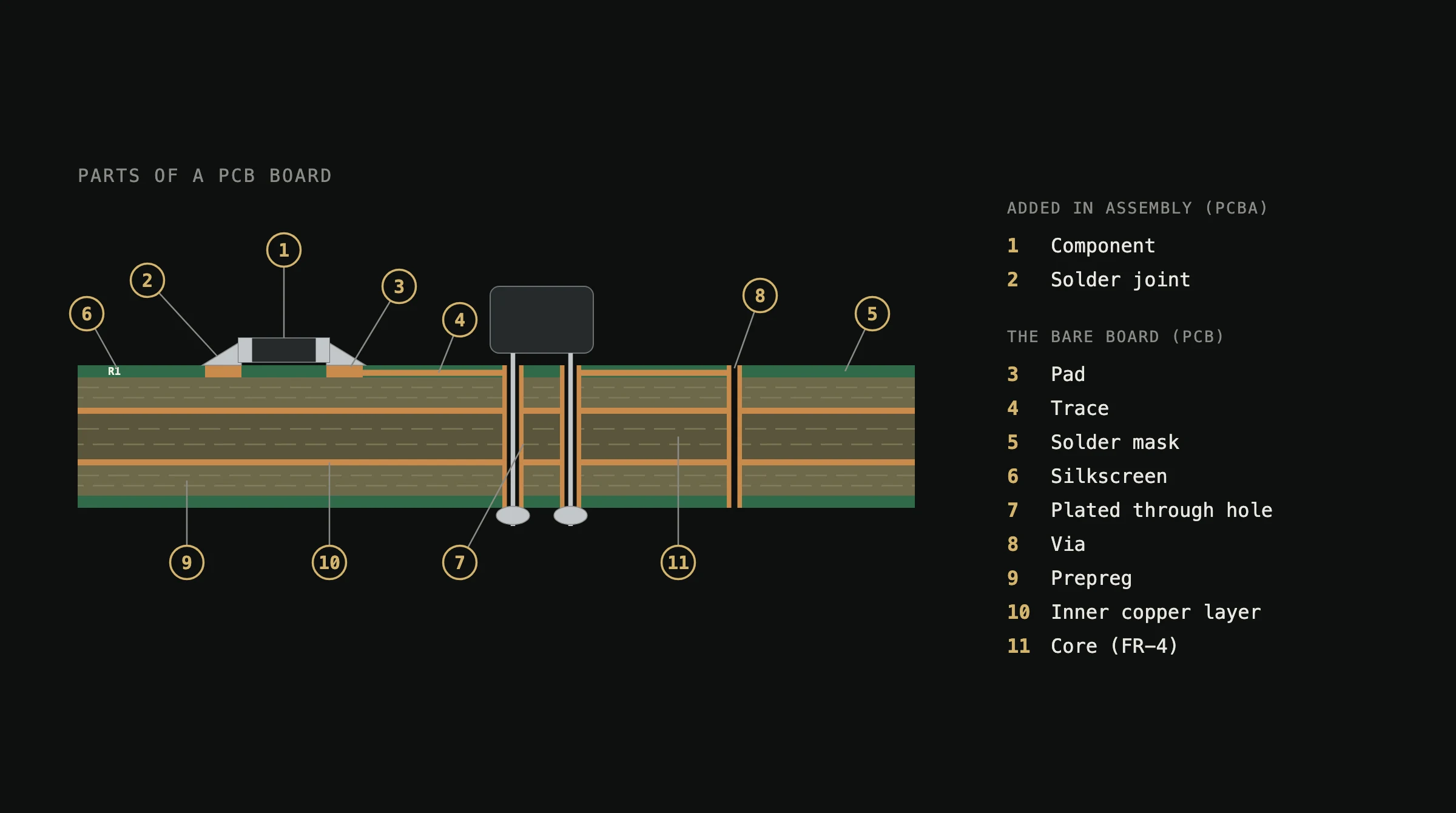
PCB diagram: the parts of a PCB board
The diagram shows a four-layer board in cross-section. Parts 1 and 2 are added when the board is assembled; parts 3 to 11 make up the bare board that a PCB plant delivers.
Added in assembly (PCBA)
- 1Component: here a surface-mount resistor, with a through-hole part to its right. Components are added in assembly.
- 2Solder joint: the metal that fixes a component to its pad and carries the current.
The bare board (PCB)
- 3Pad: exposed copper where a component is soldered, coated with a surface finish such as ENIG or HASL.
- 4Trace: a copper track that carries signals or power between pads.
- 5Solder mask: the protective coating, usually green, over all copper except the pads.
- 6Silkscreen: printed letters and outlines that mark the parts, such as R1 or U1.
- 7Plated through hole: a drilled hole lined with copper; a component lead is soldered through it.
- 8Via: a small plated hole that connects copper layers and holds no component.
- 9Prepreg: glass-fibre cloth soaked in resin; it bonds the layers and insulates them.
- 10Inner copper layer: a buried circuit or ground plane inside a multilayer board.
- 11Core: a cured laminate, usually FR-4 glass and epoxy, that gives the board its strength.
What a board is made of
Most boards start from FR-4, a glass-reinforced epoxy laminate with high dielectric strength, a UL 94 V-0 flammability rating and a good strength-to-weight ratio.[3] Copper foil on its faces is etched into the circuit. A multilayer board is built by lamination: copper foil, prepreg and inner-layer cores are bonded under controlled temperature and pressure.[4] The finished board is then covered with solder mask, given a surface finish on its exposed pads and printed with a silkscreen legend.[4]
| Layer | Material | What it does |
|---|---|---|
| Core | FR-4 glass and epoxy laminate | Gives the board its strength and insulates the copper layers |
| Copper | Copper foil | Carries signals and power as traces, pads and planes |
| Prepreg | Glass cloth soaked in resin | Bonds the layers of a multilayer board together |
| Solder mask | Polymer coating, usually green | Protects the copper and stops solder from bridging |
| Surface finish | ENIG, HASL, OSP and others | Keeps the exposed pads solderable |
| Silkscreen | Printed ink | Marks part numbers and outlines |
Main types of PCB
Boards are sorted first by how many copper layers they carry. A single-sided board has one copper layer, a double-sided board has copper on both faces of one substrate, and a multilayer board stacks several.[2]
| Type | Construction |
|---|---|
| Single-sided | One copper layer on one face of the substrate |
| Double-sided | Copper on both faces of one substrate layer |
| Multilayer | Three or more copper layers laminated into one board |
| HDI (high-density interconnect) | Fine lines and laser-drilled microvias for dense designs |
| Flexible and rigid-flex | Polyimide film that bends, alone or joining rigid sections |
High-density interconnect boards connect their layers with microvias, tiny holes drilled with a laser through a thin dielectric layer.[6] In a rigid-flex board, one or more flexible polyimide foils are pressed into the whole structure and connect the rigid parts, so a board can fold into a tight space.[7]
PCB, PCBA and the microchip
A bare printed circuit board carries no components. PCB assembly is the process of populating the board with all the components it needs,[5] and the result is called a PCBA, a printed circuit board assembly. A microchip is a third thing: a complete electrical circuit formed on a single silicon chip,[8] which is then packaged and soldered onto a board. The MPBxChange article on PCB materials draws the two side by side.
How a board is made
A typical multilayer board passes through these steps:[4]
- The circuit pattern of each inner layer is imaged onto copper-clad laminate and the unwanted copper is etched away.
- The inner layers are stacked with prepreg and copper foil and laminated under heat and pressure.
- Holes are drilled and their walls plated with copper to connect the layers.
- The outer layers are imaged, plated and etched.
- Solder mask, the surface finish and the silkscreen legend are applied.
- Each board is tested electrically and inspected.
The records a buyer can ask a plant for at each of these stages are set out in What to ask a PCB factory for.
History of the printed circuit board
| Year | Development |
|---|---|
| 1903 | Albert Hanson files a British patent for cable conductors held on layers of paper insulation |
| 1925 | Charles Ducas patents printing a conductive circuit pattern onto a supporting surface |
| 1936 to 1942 | Paul Eisler experiments with printed circuits in London and builds a radio with them |
| 1945 | Printed circuits enter mass production in a radio proximity fuze |
| 1949 to 1956 | The US Army Signal Corps "Auto-sembly" process, patented in 1956 |
| 1953 | Boards with plated through holes are developed |
| 1963 | A patent describes multilayer boards joined by plated-through holes |
| 1984 to 1991 | Laser-drilled HDI boards reach production in the United States and Japan |
| 1994 | Surface mounting accounts for about 75% of packaged chips shipped |
Albert Hanson's British patent, filed in 1903, describes conductors, bare or thinly varnished, held on a layer of paper or similar insulating material.[9] In 1925 Charles Ducas patented a method of printing a conductive layer onto a supporting surface in the form of an electrical circuit.[10]
Paul Eisler, an Austrian refugee in London, built a radio with printed circuits in 1942 after experiments that began in 1936.[12] His US patent, granted in 1948, covers producing metal conductors in position on their insulating support by a process based on printing.[11] A 1947 report of the US National Bureau of Standards records that printed circuits were introduced into mass production early in 1945, in the radio proximity fuze for mortar shells that the Bureau had developed.[13]
After the war, two Signal Corps scientists, Moe Abramson and Stanislaus Danko, developed the "Auto-sembly" process in 1949, which punched holes in a board for the component leads.[14] Their patent, granted in 1956, solders every component at once by dipping the patterned face of the board in a solder bath.[15] A 1993 Dataquest report dates the board with plated through holes to 1953, when it replaced the hand-wiring of circuits.[16] By the early 1960s patents described multilayer boards: stacks of insulating sheets carrying conductors and joined by continuously plated-through holes.[17]
Two later changes shaped today's boards. Surface-mount technology placed components on the board's surface; by 1994 it accounted for about 75% of packaged chips shipped, and through-hole mounting for 17%.[18] High-density boards with laser-drilled microvias appeared in 1984 with Hewlett-Packard's computer boards and in 1991 in Japan with Surface Laminar Circuits.[19]
PCBs in Thailand
Board making in Thailand dates back at least to the 1980s. KCE Electronics was established on 5 November 1982 and listed on the Stock Exchange of Thailand in August 1988.[20] Fujikura's printed circuit business set up its Thai plant in Navanakorn in 1988.[21]
The industry has grown fastest in recent years. TPCA puts Thailand's PCB production value at US$5.06 billion in 2025, 22.4% more than the year before and about 5.4% of world production.[22] The MPBxChange register lists 39 PCB plants in Thailand, 33 of them operating or ramping up. Their owners, sites and pipeline are covered in Thailand's PCB build-out.
Data and method
This note draws on public sources opened on 15 October 2026: patent records on Google Patents, museum and archive collections, a US government report of 1947, archived Dataquest market reports, company investor pages, PCB manufacturers' technical pages and trade press. Dates are those each source gives. Where sources describe the wartime fuze differently, the note reports the wording of the 1947 National Bureau of Standards report. The cross-section of a board is a schematic drawn by MPBxChange; its proportions are illustrative.
Sources
- company Zachariah Peterson (2020). What is a PCB and Intro to PCB Design. Altium. back to text
- company The Sierra Circuits Team (2019). What is a PCB?. Sierra Circuits. back to text
- company Milan Yogendrappa (2021). Why FR4 Material is Commonly used in PCB Fabrication?. Sierra Circuits. back to text
- company Sierra Circuits (2025). PCB Manufacturing Process. Sierra Circuits. back to text
- company Sierra Circuits (2021). PCB Assembly Process. Sierra Circuits. back to text
- company Würth Elektronik (2026). HDI Microvia PCBs. Würth Elektronik eiSos GmbH & Co. KG (we-online.com). back to text
- company Würth Elektronik (2026). RIGID.flex PCB solutions. Würth Elektronik eiSos GmbH & Co. KG (we-online.com). back to text
- academic Computer History Museum (2026). 1959: Practical Monolithic Integrated Circuit Concept Patented. Computer History Museum (The Silicon Engine). back to text
- official Albert Parker Hanson (1903). Improvements in or connected with Electric Cables and the Jointing of the same (GB190304681A). Google Patents. back to text
- official Charles Ducas (1925). Electrical apparatus and method of manufacturing the same (US1563731A). Google Patents. back to text
- official Paul Eisler (1948). Manufacture of electric circuit components (US2441960A). Google Patents. back to text
- academic Science Museum Group (2026). Radio set containing original printed circuit boards. Science Museum Group Collection. back to text
- official Cledo Brunetti and Roger W. Curtis (1947). Printed Circuit Techniques (National Bureau of Standards Circular 468). National Bureau of Standards, US Department of Commerce (hosted by NIST). back to text
- official Susan Thompson, CECOM Command Historian (2026). Historical Innovations pave the way for current microelectronic mission at CECOM. U.S. Army (army.mil). back to text
- official Moe Abramson and Stanislaus F. Danko (1956). Process of assembling electrical circuits (US2756485A). Google Patents. back to text
- data Dataquest Incorporated (1993). Integrated Circuit Packaging Trends Focus Report. Dataquest (archived by the Computer History Museum). back to text
- official Donald E. Bedson, Salvatore A. Di Nuzzo and Anthony C. Suleski (Hazeltine Research, Inc.) (1963). Multiplanar printed circuits and methods for their manufacture (US3102213A). Google Patents. back to text
- data Dataquest Incorporated (1995). Integrated Circuit Packaging Focus Report. Dataquest (archived by the Computer History Museum). back to text
- company Happy Holden (2019). Get to Know Microvia Manufacturing Processes and HDI Substrates. Altium. back to text
- company KCE Electronics Public Company Limited (2026). Company's Business. KCE Electronics (investor relations website). back to text
- company Fujikura Printed Circuits Ltd. (2023). History | Corporate information for Fujikura Printed Circuits Ltd.. Fujikura Printed Circuits Ltd.. back to text
- data TPCA (Taiwan Printed Circuit Association) (2026). AI, Geopolitics Drive Southeast Asia's High-End PCB Ecosystem. I-Connect007 (IPC Publishing Group Inc.). back to text
How to cite: MPBxChange (2026). What is a PCB board? The circuit board explained, with its history. MPBxChange research. https://www.mpbxchange.com/research/what-is-a-pcb-board-printed-circuit-board-history