Research on printed circuit boards grew from 608 journal articles in 2015 to 984 in 2025, and the fastest-growing topic was teaching computers to find defects: from 3 papers in 2015 to 94 in 2025.[57] This review reads the peer-reviewed work of 2024 to 2026 on five fronts that matter to anyone who designs, buys or makes boards: machine inspection, glass cores and low-loss materials for AI hardware, heat and reliability, greener boards, and what happens to boards at the end of their life. The short answer is that the evidence is younger than the headlines. Most results come from laboratories, simulations or a single production line, and several of the most-quoted numbers shrink when tested on real factory data.
- 2Chip and package substrateGlass cores replace organic cores under large AI chips: flatter for the chip, harder on the joints below.
- 3Solder jointsFatigue from heat cycles and vibration; underfill helps one and hurts the other.
- 2Laminate: resin, glass cloth, copper foilLower-loss resins, low-Dk glass fibre and smoother copper for 112G and 224G signals.
- 3Microvias and plated holesStacked microvias fail at the plated interface; process quality matters more than the drawing.
- 3Heat pathCopper inlays, metal cores and in-board vapour chambers cut thermal resistance by a third or more.
- 1Inspection on the lineAI filters false alarms from optical inspection; benchmark scores overstate field accuracy.
- 4Materials and makingRecyclable laminates, bio-based substrates and cleaner power at the plant.
- 5End of lifeMetal recovery from scrap boards, and the health cost of burning them in the open.
Key points
- AI inspection works best where it is least advertised. Papers routinely report 95 to 99% scores on public test sets, but the most cited set holds 693 photographs of boards with artificially made defects.[2] On one real assembly line, a model trained to recheck the inspection machine's alarms caught 74 to 88% of true defects on boards it had not seen before, and cut human rechecking by more than 98%.[6]
- Glass cores trade one problem for another. Glass under large AI chips keeps the chip side flat, but a model by a leading substrate maker puts strain in the joints below at more than twice the level of an organic core.[12] Cracking, not signal loss, is the main risk in every reliability study reviewed.[11][15][17]
- There is no peer-reviewed measurement of loss per inch on a complete 224G board. Published material work reports loss at 10 GHz on resins and bulk glass; board-level figures for the fastest links still come from vendors.[20][21][22]
- Reinforcing a joint can shorten its life. In one study, underfill raised vibration life 84 times and cut life under heat cycles by 92%.[27] What protects a car module can harm a server board.
- A recyclable FR-4 now exists outside the laboratory. A laminate from a major Chinese copper-clad laminate maker meets the industry laminate standard and holds a UL listing; its recycled resin is reused only in a lower-grade board.[36]
- Greener materials shift burdens. A bio-based substrate cut its carbon footprint by 72% and raised land use 332% and water use 465%.[39] On complex boards, the chips and the plant's electricity matter more than the laminate.[41][42]
- Smelting still beats the new chemistry on a fossil-fuel grid,[44] and Thai field studies show soil at the Kalasin e-waste site above international limits, with contamination rising over time.[50]
- All articles on printed circuit boards608 2015 · 984 2025
- Defect detection3 2015 · 94 2025
- Thermal management3 2015 · 17 2025
- Glass core substrates0 2015 · 16 2025
- Life cycle assessment1 2015 · 5 2025
Show the numbers
| 2015 | 2016 | 2017 | 2018 | 2019 | 2020 | 2021 | 2022 | 2023 | 2024 | 2025 | |
|---|---|---|---|---|---|---|---|---|---|---|---|
| All articles on printed circuit boards | 608 | 585 | 640 | 677 | 721 | 743 | 767 | 815 | 894 | 930 | 984 |
| Defect detection | 3 | 2 | 4 | 6 | 4 | 10 | 18 | 28 | 31 | 67 | 94 |
| Thermal management | 3 | 4 | 3 | 3 | 7 | 11 | 11 | 11 | 5 | 8 | 17 |
| Glass core substrates | 0 | 0 | 0 | 3 | 0 | 0 | 3 | 1 | 2 | 2 | 16 |
| Life cycle assessment | 1 | 1 | 3 | 0 | 0 | 0 | 1 | 0 | 1 | 3 | 5 |
How this review was done
This is a narrative review, written to the standards of a journal article but for a general reader. Scopus and Web of Science were not used directly. Papers were found through OpenAlex, which indexes the journals both databases cover, and cross-checked in Crossref and Semantic Scholar. Open full texts were read through Unpaywall and PubMed Central where they existed; otherwise the abstract was used, and the text says so where it matters.
- Period: published January 2024 to 21 October 2026.
- Included: peer-reviewed journal articles, and a small number of papers from the Electronic Components and Technology Conference (ECTC) and the IMAPS symposium where the journal literature on a topic is thin. Preprints, theses, vendor white papers and press reports were excluded.
- Themes: chosen by where publication counts grew fastest, shown above, and by what matters to buyers and to Thailand.
- Checks: every paper's DOI, authors, journal, volume and year were confirmed in Crossref on 22 October 2026, and none carries a correction or retraction notice. Each source below quotes the sentence that supports the claim it is attached to.
- Selection: within each theme, the most cited recent work, the largest or most rigorous studies, at least one review, and results that contradict common practice. More than 60 papers were screened in full text or abstract; 56 are cited.
Where a paper comes from a company with an interest in the result, or from a publisher whose review standards vary, the text says so.
1. AI inspection: the 98% problem
Bare-board and assembly lines already rely on automated optical inspection (AOI) and X-ray. What changed after 2023 is the volume of papers proposing deep-learning detectors, almost all of them variants of the YOLO family of object-detection models. The most cited, YOLO-HMC, reports a mean average precision (mAP) of 98.6%.[1] CDI-YOLO reports 98.3%, and its authors explain the data: 693 photographs of boards, cut into 10,668 smaller images and then split into training and test sets.[2] When images are cut before they are split, pieces of the same board can sit on both sides of the split, which flatters the score; the paper does not say which order was used. One of the few public datasets of assembled boards, PCBA-DET, holds 4,000 photographs taken by hand to imitate a line camera, with 18,100 labelled defects; its model scored 97.3%.[3] A review of the field lists nine public datasets and fourteen defect types, and names class imbalance and tiny defects as the main open problems.[5] The authors of one new dataset write that existing sets "lack comprehensive labeling".[4]
The few studies on production data tell a more useful story. One mixed-model surface-mount line in China supplied 34,466 images that the AOI machine had flagged, from 26,266 boards; only 175 were real defects, about one for every 196 alarms.[6] A classifier trained to recheck those alarms caught 78 to 89% of real defects at two settings. Tested only on boards it had never seen, recall fell to 74 and 88%, which shows how a careless split inflates results. Manual rechecking fell by more than 98%. The paper is from a single line, its first author also works for a technology company, and it was reviewed and accepted within five weeks in an MDPI journal, so it needs repeating elsewhere.
Other line studies are smaller. A pipeline that combined a vision model with GPT-4o found missing parts with 91.7% accuracy on a live surface-mount line.[7] An X-ray method for solder bridges under ball-grid arrays reported 92.6% recall, on a test set of 11 images.[9] And detectors trained on ordinary photographs lost much of their accuracy on X-ray images, and needed adapting to work across X-ray machine settings.[8] A review written from Malaysia notes that the physics, shape and size of solder joints remain under-addressed in vision research.[10]
Public benchmark datasets
Production data
What it means for buyers. A supplier's claim of "AI inspection" says little until it comes with numbers from its own line: how many alarms per thousand boards, what share are false, and how many defects escape to the customer. No paper reviewed here links AI inspection to returns or field failures.
2. Glass cores and low-loss materials for AI hardware
The largest AI processors are mounted on package substrates up to 100 mm across, and organic cores warp at that size. Glass is flat, stiff and smooth, and its expansion with heat can be tuned. Papers on glass core substrates rose from 2 in 2024 to 16 in 2025.[57]
A review from Binghamton University names the obstacles plainly: glass is fragile, cracks under stress, and long-term reliability data are scarce.[11] The tests published since bear that out.
- Cracking without a buffer. Dai Nippon Printing put glass core panels through 1,000 thermal shock cycles from minus 55 to 125 °C. Without a resin buffer layer the glass cracked; with one, nothing failed.[15] The same group measured the loss through a glass via section at 30 GHz at 0.23 dB.[16]
- Ageing. Copper-filled glass vias held at 250 °C lost most of their hardness, and the glass developed microcracks after 1,008 hours.[17]
- The board side. Georgia Tech mounted 100 mm glass packages on circuit boards, tested them through thermal cycling and found "reliability concerns persist, both with and without underfill".[14]
- The joints below. A finite-element model by engineers at Unimicron, a substrate maker, found that glass reduces strain in the chip's microbumps but more than doubles it in the joints between chip and substrate, and increases warpage at both 85 and minus 40 °C.[12][13]
- Low loss has a cost. Because glass absorbs so little energy, it also damps little: measured glass packages showed sharp resonances and power-delivery impedance peaks.[18] A 28 GHz antenna made entirely of glass measured only 0.021 dB per mm of line loss, yet its edges cracked when connectors were tightened.[19]
On the board itself, the race for faster signals has moved into the materials. New alkali-free glass fibres reach a dielectric constant of 4.5 and a loss of 0.0029 at 10 GHz, against 6.9 and 0.007 for ordinary E-glass.[20] Laboratory resins report losses of 0.0044 for a modified polyphenylene oxide composite[21] and below 0.001 for a new polyphenylene sulfide resin.[22] A simulation shows conductor loss at 40 GHz rising about 15% as copper roughness goes from 0.4 to 2.0 µm, the physics behind the demand for very smooth copper foil.[23]
Package warpage, size in micrometres (simulation)
Glass fibre dielectric constant (Dk) at 10 GHz: lower is better for fast signals
What the evidence does not show. No peer-reviewed study in this period measures loss per inch at the 28 and 56 GHz frequencies of 112G and 224G links on a complete board built from these materials. Loss figures quoted for such boards come from laminate makers and trade press. Most glass core results are conference papers or vendor tests, and none of the fabrication described is in Southeast Asia.
3. Heat and reliability
Boards for AI servers, electric vehicles and lighting carry more power in less space, and two kinds of stress decide their life: repeated heating and cooling, and vibration.
Joints and vias. A widely cited review finds that solder joint cracks start along the boundary between the solder and the intermetallic layer, and that solder thickness and the time held hot matter less than often assumed.[24] For stacked microvias, the rule of thumb has been to avoid stacking them. A 2026 modelling study from the University of Maryland's CALCE centre shows how stacked vias separate at the plated interface,[25] and a critical review argues that reliability is now governed by that hidden interface, set by drilling, cleaning and plating, more than by the geometry that standards check.[26] Both are modelling and review work, not new test campaigns.
The underfill trade-off. In a study of nine assemblies with tin-lead solder, filling under a component cut its simulated life under heat cycles by 92.3% and raised its life under vibration 84 times; fixing only the corners cut thermal life by 99.3%.[27] The test boards confirmed where cracks formed, but the lives themselves are simulated. Vehicle measurements by NXP show why the choice depends on the product: road surface and mounting position drive board vibration, and laboratory tests on bare boards fail earlier than the same parts tested in a module.[32][33]
Prediction from data. Machine-learning models trained on 185 thermal cycling tests from one laboratory predicted the characteristic life of solder joints with errors typically below 3%, better than empirical formulas and finite-element models on the same data.[28] No study shows such a model working on another laboratory's tests or on field returns.
Taking heat out. Embedding a copper inlay under silicon carbide power transistors in an EV charger cut thermal resistance by more than 30% against thermal vias, in simulation, and the prototype matched the predicted hot spots.[29] A vapour chamber built into the board reached 35% of the thermal resistance of plain FR-4 at up to 16 W.[30] On one test rig, the same LED ran with 44 °C/W of thermal resistance on FR-4, 25 on a metal-core board and below 10 on silicon-based substrates.[31] The longest test found, 8,000 hours on LEDs mounted on metal-core boards, saw little change where the LEDs stayed within rating, and failures from lens cracking and solder damage at 85 and 105 °C.[34]
Thermal resistance from one LED to its substrate, °C/W: lower runs cooler
Reinforcing a solder assembly: life under heat cycles against life under vibration (simulated)
| Heat-cycle life | Vibration life | |
|---|---|---|
| Underfill | -92.3% | 84 times |
| Corner bonding | -99.3% | 3.9 times |
What the evidence does not show. None of these papers reports failure rates of boards in service, and conductive anodic filament growth and plated-hole cracking, two classic board failures, have almost no journal literature in this period.
4. Greener boards
Two routes are being tested: boards whose materials can be recovered, and boards made from renewable materials or with less waste.
Recyclable laminates. In 2024 a team from the University of Washington and Microsoft made circuit boards from a vitrimer, an epoxy whose bonds can be reopened. A solvent recovered 98% of the polymer and all of the glass fibre, and a life-cycle assessment found 48% lower global warming potential over four recycling cycles.[35] The material softens at about 80 °C, well below soldering temperatures, and only one- and two-layer boards were shown. In 2026, a team including Shengyi Technology and Lenovo reported an acetal-cured FR-4 that meets the IPC-4101 laminate standard and holds a UL listing, decomposes only above 288 °C, and breaks down in acid at the end of life.[36] The recovered resin went into a lower-grade CEM-3 core rather than new FR-4, there is no published life-cycle assessment, and the authors work for the companies involved.
Bio-based and biodegradable boards. A microcontroller board on a substrate of polylactic acid (PLA) and flax fibre worked like FR-4 at low frequency, but production yield was about 50% and the substrate lost most of its strength in humidity tests.[37] Copper cladding and impregnation can keep water uptake under 2%, a step towards tropical service.[38] A cradle-to-gate assessment of this substrate found 6.7 kg of CO2 equivalent per square metre against 23.7 kg for FR-4, but land use 332% higher and water use 465% higher.[39] A Glasgow group printed zinc tracks onto a biodegradable base with 79% lower global warming potential than a copper and fibreglass board; zinc conducts less well than copper and the boards are single-layer.[40]
Where the footprint is. On a smartwatch, the chips dominate and the board material is negligible; on a TV remote control, the FR-4 board is the largest contributor.[41] A 2026 review finds that electricity supplies 80 to 95% of manufacturing emissions for multilayer boards on a fossil-heavy grid, so clean power at the plant is the largest single lever.[42] One study from a working plant, at AT&S in Austria, showed that recovering gold from plating rinse water cut climate impact by about a quarter.[43]
Carbon footprint of 1 m² of substrate, cradle to gate, kg CO2e
PLA and flax against FR-4, change by impact category
What the evidence does not show. Every life-cycle assessment reviewed was written by the developers of the material it favours. No peer-reviewed assessment uses data from a plant in Thailand or Southeast Asia, and no study tracks how many "recyclable" boards are actually collected.
5. End of life and health
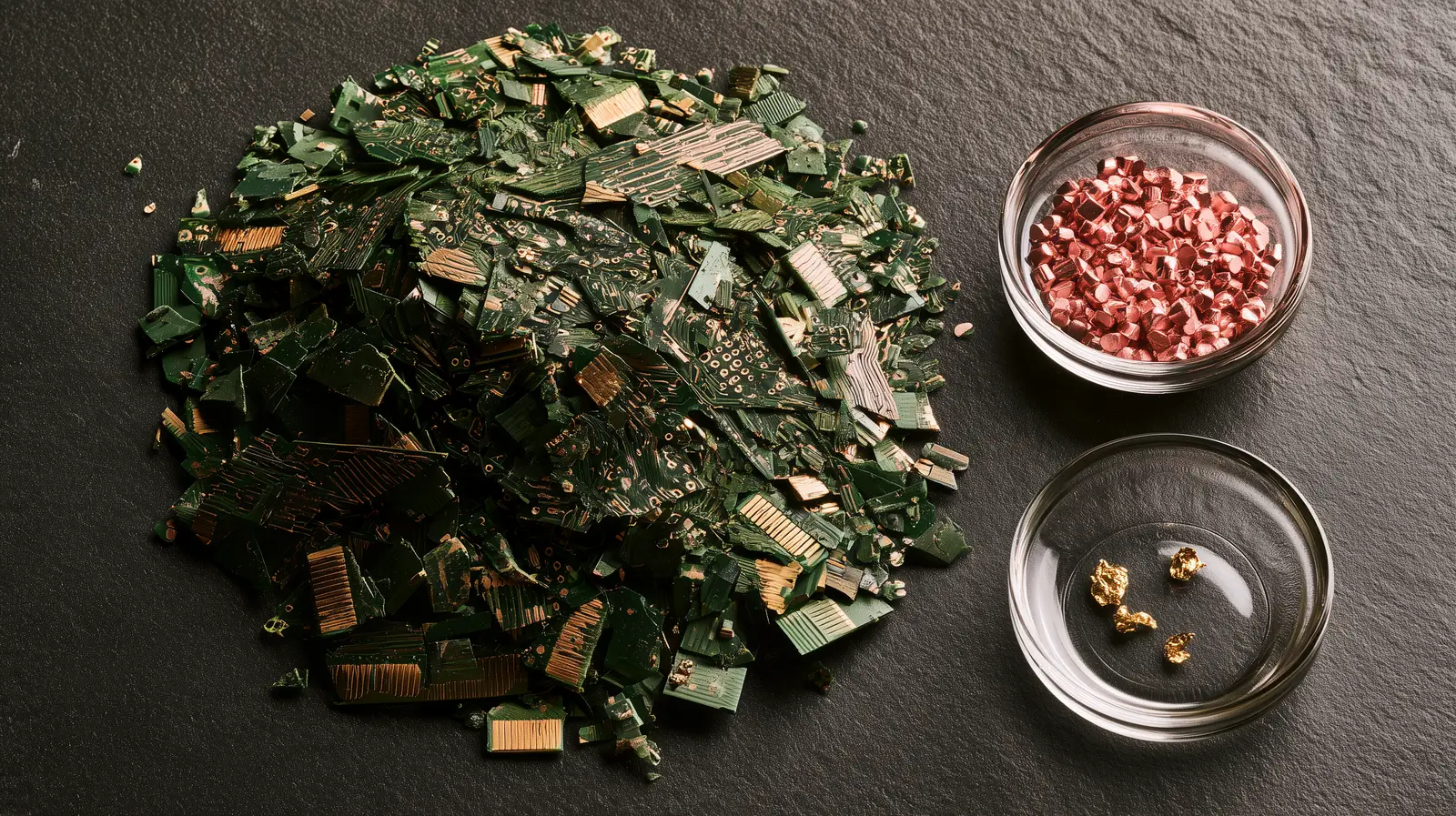
Scrap boards are valuable mainly for their gold, silver, copper and palladium, which make up more than 80% of recycling revenue while weighing 4 to 7% of the board.[48]
Which recovery route. Laboratory papers keep reporting near-complete recovery with new solvents and selective chemistry. A light-driven process recovered 8.82 g of gold from a 10 kg batch of electronic waste.[46] A review of deep eutectic solvents, a class of low-toxicity liquids, lists recoveries above 95% but notes that their viscosity, reuse and long-term stability are "under-reported".[47] The two most thorough systems studies point the other way. A comparative life-cycle assessment found that if electricity comes from fossil fuels, smelting has the lowest impact in every category studied; a combined biological and chemical route wins on global warming only with carbon-free power.[44] A study built on data from one Chinese smelter found electricity to be the main source of impact, and a 4.7-year payback for combining a switch of fuel with power generation from waste heat.[45]
Health in Thailand. Northeast Thailand now has its own evidence.
- Kalasin. At the province's largest illegal e-waste dumpsite, nickel, lead, copper, zinc and cadmium in soil exceeded United Nations Environment Programme and WHO/FAO limits, and most levels rose between 2018 and 2020.[50] Brominated flame retardants were higher in soil, food and workers' blood at e-waste sites than at control sites.[49] Several authors of that study work for environmental organisations.
- Ubon Ratchathani. Two studies in Ubon Ratchathani found no significant difference in blood or urinary lead between e-waste workers and neighbours.[51][52] More workers had lead above the detection limit (9.1% against 1.8%), and the comparison groups live nearby, so the result does not show the work is safe. In Bangladesh, by contrast, workers' median blood lead was more than three times that of other people.[53]
- A simple fix. In Kalasin, a dismantling tool designed with the workers cut self-reported injuries by 58% over three months, in a trial of 89 people.[54]
Factory wastewater. Two studies of PCB plants in southern China found that copper drives the acute toxicity of untreated wastewater and that treatment removes it well, but per- and polyfluorinated substances (PFAS) and flame retardants pass through treatment in part.[55][56] One flame retardant reached an ecological risk quotient of 20 despite its low concentration.[56] No comparable peer-reviewed study of PCB plants in Thai industrial estates was found.
E-waste workersComparison group
- Bangladesh, blood lead, median (µg/dL)
- Ubon Ratchathani, blood lead, mean (µg/dL)
- Ubon Ratchathani, urinary lead, median (µg/g creatinine)
How strong is the evidence?
| Line of work | Laboratory | Prototype or vendor test | One real line or plant | Qualified product |
|---|---|---|---|---|
| 1 AI defect detection on public benchmarks | ||||
| 1 AI filtering of inspection false alarms | ||||
| 2 Glass core substrates | ||||
| 2 Ultra-low-loss resins and glass fibres | ||||
| 3 Copper inlays and in-board vapour chambers | ||||
| 3 Machine learning for solder joint life | ||||
| 4 Recyclable acetal FR-4 laminate | ||||
| 4 Vitrimer boards | ||||
| 4 Biodegradable PLA and flax boards | ||||
| 5 Selective gold recovery by light | ||||
| 5 Smelting with waste-heat power |
Most of the work reviewed is in the laboratory or at prototype stage. Three lines have reached a real production setting: AI filtering of inspection alarms, an acetal FR-4 laminate qualified to the industry standard, and smelting with waste-heat recovery. Each rests on a single plant or company.
What it means for buyers in Thailand
On MPBxChange's reading of the evidence, five questions are worth asking a board supplier:
- Inspection. What are your false-call and escape rates per thousand boards, measured on your own line, and how do you recheck alarms?
- High-speed boards. For 112G and 224G designs, can you show measured loss per inch on a test coupon built from the laminate, glass cloth and copper you will use?
- Reliability. For stacked microvias, can you show interconnect stress test or reflow coupon results, and how do you control the plated interface? For assemblies, is underfill chosen for heat cycles or for vibration?
- Footprint. Where does your electricity come from, and do you have a product carbon footprint to ISO 14067?
- Waste. Where do your copper-bearing wastewater sludge and scrap boards go, and is PFAS measured in your effluent?
Limits of this review
This is a narrative review, not a systematic one: there was no pre-registered protocol, no second screener and no pooled statistics. Scopus and Web of Science were not searched directly. Several papers could be read only as abstracts, and their detailed numbers were not checked against full texts. Publication counts are keyword matches and include some unrelated uses of the words. The review covers English-language journals; Chinese, Japanese, Korean and Thai literature is under-represented.
Disclosure. MPBxChange runs a marketplace for PCB plants in Thailand and has an interest in buyers sourcing from them. No funding was received for this review, and no author or company named in it was contacted. AI tools assisted the literature search and first drafting; every source was checked against its DOI record, and the author is responsible for the text.
Sources
- academic Yuan, M.; Zhou, Y.; Ren, X. et al. (2024). YOLO-HMC: An Improved Method for PCB Surface Defect Detection. IEEE Transactions on Instrumentation and Measurement, 73, 1 to 11. Institute of Electrical and Electronics Engineers (IEEE). DOI 10.1109/TIM.2024.3351241. back to text
- academic Xiao, G.; Hou, S.; Zhou, H. (2024). PCB defect detection algorithm based on CDI-YOLO. Scientific Reports, 14(1), 7351. Springer Science and Business Media LLC. DOI 10.1038/s41598-024-57491-3. back to text
- academic Shen, M.; Liu, Y.; Chen, J. et al. (2024). Defect detection of printed circuit board assembly based on YOLOv5. Scientific Reports, 14(1), 19287. Springer Science and Business Media LLC. DOI 10.1038/s41598-024-70176-1. back to text
- academic Kumar Ancha, V.; Sibai, F. N.; Gonuguntla, V. et al. (2024). Utilizing YOLO Models for Real-World Scenarios: Assessing Novel Mixed Defect Detection Dataset in PCBs. IEEE Access, 12, 100983 to 100990. Institute of Electrical and Electronics Engineers (IEEE). DOI 10.1109/ACCESS.2024.3430329. back to text
- academic He, Z.; Lian, Y.; Wang, Y. et al. (2025). A comprehensive review of research on surface defect detection of PCBs based on machine vision. Results in Engineering, 27, 106437. Elsevier BV. DOI 10.1016/j.rineng.2025.106437. back to text
- academic Tian, K.; Niu, Z. (2026). A Deep Learning Approach for Automated Re-Inspection of False Calls in Mixed-Production Surface Mount Lines Under Extreme Class Imbalance. Applied Sciences, 16(20), 10068. MDPI AG. DOI 10.3390/app162010068. back to text
- academic Zhao, W.; Gomez, S.; Farrapo, B. et al. (2026). Towards autonomous PCB manufacturing: an AI-powered automatic optical inspection framework. Manufacturing Letters, 49, 1519 to 1529. Elsevier BV. DOI 10.1016/j.mfglet.2026.08.057. back to text
- academic Nguyen, H. D.; Cheng, D.; Wang, X. et al. (2025). Data-Efficient Deep Learning for Printed Circuit Board Defect Detection Using X-Ray Images. IEEE Transactions on Instrumentation and Measurement, 74, 1 to 14. Institute of Electrical and Electronics Engineers (IEEE). DOI 10.1109/TIM.2025.3529089. back to text
- academic Zhou, X. (2026). An industrial X-ray inspection framework for SMT solder bridge detection in BGA assemblies. The International Journal of Advanced Manufacturing Technology, 143(11-12), 7373 to 7378. Springer Science and Business Media LLC. DOI 10.1007/s00170-026-17943-8. back to text
- academic Ong, T. Y.; Tan, K. T.; Teoh, P. C. et al. (2025). Review of solder joint vision inspection for industrial applications. The International Journal of Advanced Manufacturing Technology, 137(7-8), 3257 to 3272. Springer Science and Business Media LLC. DOI 10.1007/s00170-025-15383-4. back to text
- academic Lai, Y.; Pan, K.; Park, S. (2024). Thermo-mechanical reliability of glass substrate and Through Glass Vias (TGV): A comprehensive review. Microelectronics Reliability, 161, 115477. Elsevier BV. DOI 10.1016/j.microrel.2024.115477. back to text
- academic Lau, J. H.; Liu, N.; Ma, M. et al. (2025). Solder Joint Reliability of Glass Core Substrate Assembly. IMAPSource Proceedings, 2024(Symposium). IMAPS - International Microelectronics Assembly and Packaging Society. DOI 10.4071/001c.129522. back to text
- academic Lau, J. H.; Liu, N.; Ma, M. et al. (2025). Solder joint reliability - glass core substrate versus organic core substrate. Microelectronics Reliability, 168, 115701. Elsevier BV. DOI 10.1016/j.microrel.2025.115701. back to text
- academic Lee, Y.; Godbole, K.; Park, H. et al. (2026). Board-Level Reliability of 100 × 100 mm Large Glass Packages: Warpage and Thermomechanical Reliability for AI/HPC Applications. IEEE Transactions on Components, Packaging and Manufacturing Technology, 16(2), 330 to 342. Institute of Electrical and Electronics Engineers (IEEE). DOI 10.1109/TCPMT.2025.3614186. back to text
- academic Fujimoto, K.; Kuramochi, S. (2026). Development of Long-term Reliability for Glass Core Substrates with Build-up layers. 2026 IEEE 76th Electronic Components and Technology Conference (ECTC), 815 to 819. IEEE. DOI 10.1109/ECTC51846.2026.00138. back to text
- academic Fujimoto, K.; Okawa, Y.; Tai, T. et al. (2024). Development of Glass core substrate with the stress analysis, transmission characteristics and reliability. 2024 IEEE 74th Electronic Components and Technology Conference (ECTC), 546 to 550. IEEE. DOI 10.1109/ECTC51529.2024.00093. back to text
- academic Chen, J.; Li, Z.; Yang, B. et al. (2026). Long-term high-temperature aging mechanism of copper-metallized through-glass vias: a combined nanoindentation test and hybrid Potts-phase field simulation study. Microsystems & Nanoengineering, 12(1), 46. Springer Science and Business Media LLC. DOI 10.1038/s41378-026-01160-0. back to text
- academic Kim, Y. (2025). Measurement and Analysis of Interconnects’ Resonance and Signal/Power Integrity Degradation in Glass Packages. Micromachines, 16(1), 112. MDPI AG. DOI 10.3390/mi16010112. back to text
- academic Ahn, B. K. (2026). Polymer-free all-glass millimeter-Wave antenna-in-package platform with vertical-transition-free aperture-coupled feeding at 28 GHz. Scientific Reports, 16(1), 29809. Springer Science and Business Media LLC. DOI 10.1038/s41598-026-59503-w. back to text
- academic Kadathala, L.; Park, Y. O.; Kim, J. H. et al. (2024). Low dielectric properties of alkali-free aluminoborosilicate fiber glasses for PCB applications at 10 GHz. Scientific Reports, 14(1), 27749. Springer Science and Business Media LLC. DOI 10.1038/s41598-024-79456-2. back to text
- academic Zhen, Z.; Zeng, X.; Zeng, X. et al. (2026). Oligomer engineering enabling high-performance Poly(phenylene oxide) resins for high-frequency/speed copper clad laminates. Advanced Industrial and Engineering Polymer Research, 9(1), 11 to 22. Elsevier BV. DOI 10.1016/j.aiepr.2025.09.003. back to text
- academic Ito, D.; Inoue, K.; Fujioka, Y. et al. (2025). Novel polyphenylene sulfide resin for high-frequency copper-clad laminates with low dielectric tangent and flame retardancy. Polymer, 338, 129095. Elsevier BV. DOI 10.1016/j.polymer.2025.129095. back to text
- academic Yang, Z.; Zhu, Y.; Jiang, H. et al. (2024). Effects of Non-Gaussian Surface Roughness on Conductor Loss in High-Frequency Transmission Lines. IEEE Transactions on Components, Packaging and Manufacturing Technology, 14(5), 930 to 937. Institute of Electrical and Electronics Engineers (IEEE). DOI 10.1109/TCPMT.2024.3383879. back to text
- academic Li, L.; Du, X.; Chen, J. et al. (2024). Thermal Fatigue Failure of Micro-Solder Joints in Electronic Packaging Devices: A Review. Materials, 17(10), 2365. MDPI AG. DOI 10.3390/ma17102365. back to text
- academic Abbas, S. M.; Yu, Q.; Pecht, M. (2026). Investigation of the Interface Reliability of Multilevel Stacked Copper Microvias: Modeling and Simulation. IEEE Transactions on Components, Packaging and Manufacturing Technology, 16(9), 2054 to 2067. Institute of Electrical and Electronics Engineers (IEEE). DOI 10.1109/TCPMT.2026.3704315. back to text
- academic Kamble, V. G. (2026). Interface‐Controlled Reliability of HDI Microvias: A Critical Review and Perspective. Advances in Materials Science and Engineering, 2026(1), 1189580. Wiley. DOI 10.1155/amse/1189580. back to text
- academic Tian, W.; Li, F.; He, M. et al. (2025). Reliability Analysis of Complex PCB Assemblies Under Temperature Cycling and Random Vibration. Micromachines, 16(2), 212. MDPI AG. DOI 10.3390/mi16020212. back to text
- academic Alavi, S.; Sumaiya, O.; Silva, D. F. et al. (2026). Benchmarking Machine Learning Methods Against Finite Element and Empirical Models for Predicting Solder Joint Characteristic Life. IEEE Transactions on Components, Packaging and Manufacturing Technology, 16(5), 1047 to 1061. Institute of Electrical and Electronics Engineers (IEEE). DOI 10.1109/TCPMT.2025.3614513. back to text
- academic Awais, M.; Amin, S.; Brito, F. P. et al. (2026). Thermal Management and Experimental Validation of a Copper-Inlay PCB for SiC MOSFETs in High-Power EV Fast Chargers. IEEE Open Journal of Power Electronics, 7, 1006 to 1020. Institute of Electrical and Electronics Engineers (IEEE). DOI 10.1109/OJPEL.2026.3672717. back to text
- academic Yu, J. C.; Liao, C. N.; Chang, Y. H. et al. (2024). Enhanced Heat Spreading Performance of Printed Circuit Boards by Vapor Chamber Implementation. IEEE Transactions on Components, Packaging and Manufacturing Technology, 14(2), 221 to 228. Institute of Electrical and Electronics Engineers (IEEE). DOI 10.1109/TCPMT.2024.3358867. back to text
- academic Chidambaram, N. V.; Jayalakshmi, R.; Ramachandran, C. S. et al. (2024). A Comparative Thermal and Lumen Performance Study of Thin-film Amorphous Silicon Dielectric Coating on Aluminum as an LED Packaging Substrate. Silicon, 16(11), 4831 to 4841. Springer Science and Business Media LLC. DOI 10.1007/s12633-024-03043-3. back to text
- academic Thukral, V.; Roucou, R.; Chou, C. et al. (2024). Understanding board level vibrations in automotive electronic modules. Microelectronics Reliability, 159, 115430. Elsevier BV. DOI 10.1016/j.microrel.2024.115430. back to text
- academic Thukral, V.; Chou, C.; Roucou, R. et al. (2025). Automotive Application-driven Vibration Test Approach: Bridging the Gap between Module and Board Level Reliability Test Methods. 2025 IEEE 75th Electronic Components and Technology Conference (ECTC), 362 to 369. IEEE. DOI 10.1109/ECTC51687.2025.00068. back to text
- academic Caria, A.; Fraccaroli, R.; Pierobon, G. et al. (2025). Long-term (8000 h) reliability and failures of high-power LEDs for outdoor lighting stressed at high ambient temperatures. Microelectronics Reliability, 168, 115634. Elsevier BV. DOI 10.1016/j.microrel.2025.115634. back to text
- academic Zhang, Z.; Biswal, A. K.; Nandi, A. et al. (2024). Recyclable vitrimer-based printed circuit boards for sustainable electronics. Nature Sustainability, 7(5), 616 to 627. Springer Science and Business Media LLC. DOI 10.1038/s41893-024-01333-7. back to text
- academic Mo, Y.; Lin, W.; Zhou, Y. et al. (2026). Recyclable glass fiber-reinforced epoxy copper clad laminates for printed circuit board. Communications Chemistry, 9(1), 329. Springer Science and Business Media LLC. DOI 10.1038/s42004-026-02078-4. back to text
- academic Géczy, A.; Piffkó, D.; Berényi, R. et al. (2024). Implementation of microcontroller board on a sustainable and degradable PLA/flax composite substrate: a case study. Nanotechnology, 35(43), 435201. IOP Publishing. DOI 10.1088/1361-6528/ad66d3. back to text
- academic Géczy, A.; Farkas, C.; Gyenizse, L. et al. (2026). Water uptake and dry-out properties of sustainable, flame-retarded, PLA-flax biocomposite printed circuit board substrates. Results in Engineering, 30, 110899. Elsevier BV. DOI 10.1016/j.rineng.2026.110899. back to text
- academic Lebrun, J.; Toussaint, S.; Wattiez, A. et al. (2026). Comparative cradle-to-gate life cycle assessment of conventional and bio-based printed circuit board substrates. Sustainability Science and Technology, 3(4), 044001. IOP Publishing. DOI 10.1088/2977-3504/aea32e. back to text
- academic Harwell, J. R.; Zhang, T.; Rollo, A. et al. (2025). Additively manufacturing printed circuit boards with low waste footprint by transferring electroplated zinc tracks. Communications Materials, 7(1), 17. Springer Science and Business Media LLC. DOI 10.1038/s43246-025-01031-7. back to text
- academic Zhang, T.; Bainbridge, A.; Harwell, J. et al. (2024). Life cycle assessment (LCA) of circular consumer electronics based on IC recycling and emerging PCB assembly materials. Scientific Reports, 14(1), 29183. Springer Science and Business Media LLC. DOI 10.1038/s41598-024-79732-1. back to text
- academic Negi, S.; Rani, A.; Pan, S. Y. (2026). Strategies for decarbonizing printed circuit board supply chain. iScience, 29(5), 115559. Elsevier BV. DOI 10.1016/j.isci.2026.115559. back to text
- academic Nemati, E.; Prenzel, T. M.; Lorenz, M. et al. (2026). Environmental sustainability potentials of gold recovery via membrane distillation in the production of printed circuit boards. Cleaner Environmental Systems, 21, 100425. Elsevier BV. DOI 10.1016/j.cesys.2026.100425. back to text
- academic Schwartz, E.; He, H.; Frost, K. et al. (2024). Comparative life cycle assessment of copper and gold recovery from waste printed circuit boards: Pyrometallurgy, chemical leaching and bioleaching. Journal of Hazardous Materials, 473, 134545. Elsevier BV. DOI 10.1016/j.jhazmat.2024.134545. back to text
- academic Wang, X.; Huang, W.; Yan, B. et al. (2025). E-waste recycling: Integrated life cycle assessment and techno-economic analysis unravels pyrometallurgy’s edge and delivers an optimization framework for recovering waste printed circuit boards. Waste Management, 207, 115135. Elsevier BV. DOI 10.1016/j.wasman.2025.115135. back to text
- academic Shang, H.; Chen, Y.; Guan, S. et al. (2024). Scalable and selective gold recovery from end-of-life electronics. Nature Chemical Engineering, 1(2), 170 to 179. Springer Science and Business Media LLC. DOI 10.1038/s44286-023-00026-w. back to text
- academic Moganti, L. K.; Dutta, D. (2026). Deep eutectic solvents in E-waste recycling: preparation, properties, and hydrometallurgical metal recovery. RSC Advances, 16(6), 5228 to 5251. Royal Society of Chemistry (RSC). DOI 10.1039/d5ra08854b. back to text
- academic Xia, D.; Lee, C.; Charpentier, N. M. et al. (2024). Drivers and Pathways for the Recovery of Critical Metals from Waste‐Printed Circuit Boards. Advanced Science, 11(30), 2309635. Wiley. DOI 10.1002/advs.202309635. back to text
- academic Walaska, H.; Dvorska, A.; Petrlik, J. et al. (2024). PBDEs and dechlorane plus contamination in community e-waste recycling: Environmental and health implications in Northeastern Thailand. Toxicology, 509, 153972. Elsevier BV. DOI 10.1016/j.tox.2024.153972. back to text
- academic Pokethitiyook, P.; Joradon, P.; Poolpak, T. et al. (2026). Environmental risk assessment of heavy metal and PAH contamination at Kalasin e-waste dumpsite and screening of native hyperaccumulators. Environmental Geochemistry and Health, 48(8), 381. Springer Science and Business Media LLC. DOI 10.1007/s10653-026-03272-y. back to text
- academic Sangwijit, C.; Ong-artborirak, P.; Naksen, W. et al. (2025). Health Effects of Heavy Metal Exposure Among E-waste Workers and Community-dwelling Adults in Thailand: A Cross-sectional Study. Journal of Preventive Medicine and Public Health, 58(2), 156 to 166. Korean Society for Preventive Medicine. DOI 10.3961/jpmph.24.415. back to text
- academic Harasarn, K.; Keawkaen, P.; Thetkathuek, A. (2026). Neurocognitive consequences of occupational heavy metal exposure among electronic waste sorting workers in Thailand. Narra J, 6(1), e2994. Narra Sains Indonesia. DOI 10.52225/narra.v6i1.2994. back to text
- academic Parvez, S. M.; Jahan, F.; Abedin, J. et al. (2024). Blood lead, cadmium and hair mercury concentrations and association with soil, dust and occupational factors in e-waste recycling workers in Bangladesh. International Journal of Hygiene and Environmental Health, 257, 114340. Elsevier BV. DOI 10.1016/j.ijheh.2024.114340. back to text
- academic Shkembi, A.; Linhart, E.; Chou, S. et al. (2026). Enhancing informal workers’ tools to reduce workplace injuries: a quasi-randomized control trial of electronic waste recyclers in Thailand. Scandinavian Journal of Work, Environment & Health, 52(2), 139 to 146. Scandinavian Journal of Work, Environment and Health. DOI 10.5271/sjweh.4259. back to text
- academic Zhang, L.; Xie, L.; Li, H. et al. (2026). Heavy metals or emerging organic contaminants: Which drive zebrafish embryo toxicity in printed circuit board manufacturing wastewater?. Water Research, 308, 126833. Elsevier BV. DOI 10.1016/j.watres.2026.126833. back to text
- academic Zhang, J.; Diao, J.; Jing, F. et al. (2026). Unveiling typical emerging contaminants in wastewater from printed circuit board industries in South China. Journal of Environmental Sciences, 169, 236 to 244. Elsevier BV. DOI 10.1016/j.jes.2025.11.043. back to text
- data OurResearch (2026). OpenAlex works API: journal articles a year whose title or abstract contains "printed circuit board", alone and with "defect detection", "thermal management" or "life cycle assessment", and "glass core" substrate, 2015 to 2025. OpenAlex. back to text
How to cite: Dendoung, T. (2026). What PCB research found in 2024 to 2026: inspection, glass, heat and greener boards. MPBxChange research. https://www.mpbxchange.com/research/what-pcb-research-found-2024-2026