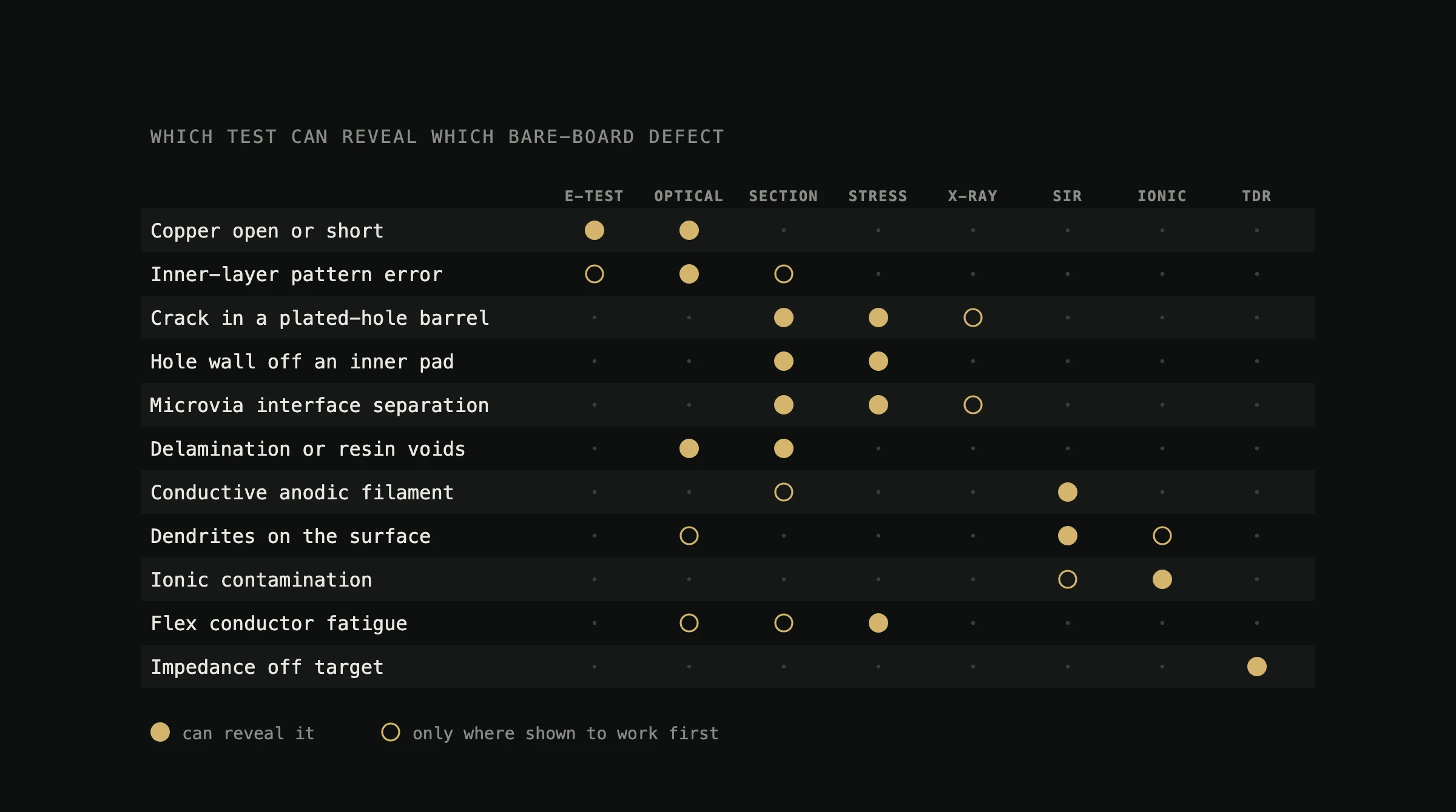
A printed circuit board can pass its final electrical test and still fail in service. Each test a plant runs answers one question: whether every net connects as the board data says, whether a layer matches its artwork, whether a plated hole survives heat, whether the surface stays insulating in humid air. This note takes eleven defects of a bare board, from opens and shorts to cracked hole barrels, filament growth inside the laminate and impedance off target, and sets out which tests can reveal each one, what a passing result leaves unproven, and which tests use up or destroy the sample.
Key points
- A final electrical test checks every net for opens and for shorts to other nets against the original board data.[1] NASA notes that this test runs to parameters set by the customer,[2] so the buyer's specification decides what it checks.
- Inner layers can only be inspected before lamination. One European fabricator gives each inner-layer panel a complete automatic optical inspection against the design data at that point.[3]
- Cracked hole barrels and holes pulled away from their inner pads are found by cycling a coupon through heat while its resistance is measured, and by cross-sections.[4] When NASA Goddard re-examined suppliers' own cross-sections, 20 to 30% were rejected.[5]
- In Isola's humidity and bias tests of laminates, insulation resistance fell and recovered after baking, but no conductive filament grew;[6] a laminate's result does not by itself cover a drilled board.
- A drop in surface insulation resistance shows that a surface leaks, not why it leaks;[7] identifying the ions on it points to the cause.
Three questions, three kinds of test
Tests on a bare board answer three different questions. The first is connectivity: does each net connect where the data says, and nowhere else? An electrical test answers it at the moment of the test. The second is conformance: does the copper look like its artwork? Optical inspection compares a layer with an image generated from the design data,[3] so it confirms that the board follows the data, not that the data is right. The third is life: how long will the board keep working through soldering heat, temperature swings, humidity or bending? Only a stress test answers that, and only for the structures it stresses.
A pass on one question says nothing about the others. A board can connect perfectly on the day it is tested and still carry a plated hole too thin to survive reflow. That is why reliability work in the sources below pairs stress with measurement while the stress is applied, then cuts the sample to see what happened.[4]
Which test reveals which defect
| Defect | E-test | Optical | Section | Stress | X-ray | SIR | Ionic | TDR |
|---|---|---|---|---|---|---|---|---|
| Copper pattern open or short | ● | ● | ||||||
| Inner-layer pattern error or narrowed conductor | ○ | ● | ○ | |||||
| Crack around a plated-hole barrel | ● | ● | ○ | |||||
| Hole wall separated from an inner pad | ● | ● | ||||||
| Microvia interface separation | ● | ● | ○ | |||||
| Delamination, resin cracks or voids | ● | ● | ||||||
| Conductive anodic filament (CAF) inside the laminate | ○ | ● | ||||||
| Dendrites and migration on the surface | ○ | ● | ○ | |||||
| Ionic contamination or residue | ○ | ● | ||||||
| Flex conductor fatigue or rigid-flex transition damage | ○ | ○ | ● | |||||
| Impedance off target or discontinuous | ● |
- Copper pattern open or short● E-test · Optical
- Inner-layer pattern error or narrowed conductor● Optical○ E-test · Section
- Crack around a plated-hole barrel● Section · Stress○ X-ray
- Hole wall separated from an inner pad● Section · Stress
- Microvia interface separation● Section · Stress○ X-ray
- Delamination, resin cracks or voids● Optical · Section
- Conductive anodic filament (CAF) inside the laminate● SIR○ Section
- Dendrites and migration on the surface● SIR○ Optical · Ionic
- Ionic contamination or residue● Ionic○ SIR
- Flex conductor fatigue or rigid-flex transition damage● Stress○ Optical · Section
- Impedance off target or discontinuous● TDR
- ● can reveal it
- ○ only where shown to work for this feature first
- E-test
- Electrical test: continuity and isolation of each net (flying probe or fixture). Probes touch the pads and can mark them.
- Optical
- Optical inspection: automated optical inspection (AOI), microscope or visual check. Leaves the board intact.
- Section
- Microsection: a cut and polished cross-section seen under a microscope. Destroys the sample.
- Stress
- Stress with monitoring: thermal, reflow or bending cycles while resistance is measured. Uses up part of the sample's life.
- X-ray
- X-ray or computed tomography (CT). Leaves the board intact.
- SIR
- Humidity and bias insulation test: surface insulation resistance (SIR) or temperature, humidity and bias. Uses up part of the sample's life.
- Ionic
- Ionic analysis: ion chromatography or a bulk ionic (ROSE) screen. Changes the sampled surface.
- TDR
- Impedance: time-domain reflectometry and transmission (TDR, TDT). Leaves the board intact.
Copper patterns: opens, shorts and narrowed conductors
At the end of production, an electrical test checks the interconnection of the board against its original data, net by net.[1] A flying probe tester needs no fixture and is quick to set up but slow, because it tests every net. A faster tester at the same fabricator builds an electronic map from a board already tested good and compares each board with that map.[1] On that route the reference is a known-good board rather than the design data itself. The same fabricator makes electrical test standard for boards of two or more layers and an option for single-sided boards.[1] NASA lists pad damage among the issues of flying-probe testers.[2]
Inner layers are checked earlier, because a mistake cannot be corrected once the multilayer is pressed together.[3] At that stage the automatic optical inspection system scans each panel in strips and compares it with an image generated from the original design data.[3]
What a pass leaves open: a conductor that is narrowed but still continuous passes an electrical test, which asks only whether the net connects. How much copper remains is shown by measuring the flagged area under a microscope or, finally, by a cross-section.
Plated holes: cracked barrels and separated inner pads
A plated through hole fails in two main ways. Barrel cracking comes from the board expanding through its thickness far more than the copper lining of the hole; inner-layer separation comes from the resin expanding sideways into the hole, which strains the joint between the barrel and the inner copper.[4] Isola gives the scale: in the Z axis the resin and glass expand 4.5 to 5 times faster than copper below the glass transition temperature, and 17 to 20 times faster above it.[8] NASA's guidance places the two failures at different times: circumferential fatigue cracking needs temperature cycling and often appears after extended use in the field, while wall-to-pad separation occurs mainly during assembly.[2]
The test built for this is interconnect stress testing: a coupon of plated holes is heated in cycles while its resistance is measured, and a failure is a 10 percent rise in the resistance of a hole.[4] In the round robin NASA cites, it detected inner-layer separation better than the older method of thermal shock followed by cross-sections.[4] The test must stay within what the board will meet. In one study NASA cites, failures at peak temperatures of 210 °C and above were judged artefacts of the test, and 190 °C was used. NASA also cites coupons that lasted 788 cycles falling to 4 after six lead-free reflow exposures at 260 °C.[4] The soldering history of a coupon therefore belongs in its test record.
Cross-sections show what happened inside a hole, in the plane that was cut. NASA Goddard re-examined microsections submitted by suppliers and rejected 20 to 30% of them on its own inspection.[5] The study covered 882 coupon submissions from 2015 to 2017, with 260 nonconformances; inner-layer separation, which NASA defines as separation of the inner-layer foil from the plated barrel and links to opens after reflow, wave soldering or rework, was among the most frequent.[5] NASA treats micro-sectioning chiefly as a way of monitoring the process rather than as a final inspection of delivered boards.[5] X-ray, in NASA's microvia study, clearly identified filled vias but was of limited value for detecting other conditions.[4]
Microvias and sequential lamination
High-density boards are built in several pressings, and each pressing heats the layers already made. Isola names the issues associated with this technology as resin cracks, delamination, resin voids and failed microvia connections, and describes how a deforming buried via pad and swelling dielectric push and pull a microvia off its landing pad.[8] NASA reproduces a 2004 failure analysis in which via plating separated from the capture pad and caused intermittent failures on boards carrying chip-scale and ball grid array packages.[2] In NASA's own test boards, cross-sections after 100 thermal cycles found failures only in 2-mil microvias.[4]
What a pass leaves open: a microvia that connects at room temperature may still be weakly bonded to its pad. Only a stress test on coupons that copy the actual via structure, monitored while it runs and followed by cross-sections, addresses that.
Inside the laminate: delamination, voids and filament growth
Delamination and resin voids form during lamination and are driven by design as well as process: Isola reports that areas with little retained copper make up most delamination-prone designs.[8] A blister on the surface is visible; separation inside the board is found by cross-sections. Scanning acoustic microscopy, which images the inside of electronic packages, helps little here: NASA notes that the copper of a board hinders its internal examination and calls the method not practical for looking inside a printed wiring board.[5]
Conductive anodic filament (CAF) is the growth of copper inside the board, typically bridging two conductors held at opposite bias.[6] Isola's paper sets out that the time to failure depends on bias voltage, relative humidity, the spacing between holes and between lines, temperature and the resin system, and that hole-to-hole is the most common path.[6] Its tests varied resin, glass, solder mask, spacing and bias at controlled humidity. Insulation resistance dropped, more so with solder mask, but no filament grew: even at 100 volts and 12 mil between holes, the drop was reversible and baking restored it.[6] The authors point to drilling, mechanical stress and thermal shock in board fabrication as possible keys to real failures.[6] A CAF result for a laminate therefore does not show how a board drilled and pressed at a particular plant will behave; that needs a humidity and bias test on coupons from that plant's process.
On the surface: residues and dendrites
On a board under voltage in humid air, metal can dissolve at one conductor, migrate and deposit at the other, growing dendrites; failure follows when a dendrite bridges the gap and shorts the conductors.[9] The standard way to look for this risk is a surface insulation resistance (SIR) test: comb patterns are held in a climate chamber under bias and their resistance is read throughout.[7] In the National Physical Laboratory's study the combs had a 0.2 mm gap and were held at 40 °C and 93% relative humidity under 5 volts for 72 hours, read every 15 minutes.[9] Dendrite formation depended strongly on the level of flux residue, and in that study bare copper formed dendrites less readily than ENIG, whose dendrites were mainly nickel; it was one comparison under deliberate contamination, not a general ranking of finishes.[9]
An SIR result is a single number for the whole pattern: NPL notes that the measurement gives only the total resistance of the system.[9] ZESTRON makes the same point from the other side: a failed SIR value does not show why it failed, while the hygroscopy of ionic residues strongly affects surface resistance, so identifying which ions are present by ion chromatography points to the cause.[7] A bulk ionic screen averages the whole board, so a local residue can hide in a clean average.
Flexible and rigid-flex boards
A flexible circuit that is bent once to fit its housing and one that flexes in use are different products. Würth Elektronik asks the buyer to state whether the application is static or dynamic and to give the bending radii, the ratio of radius to flex thickness, the bending shape, the number of bending cycles and the bending frequency, and it refers dynamic bending applications to its specialists.[10] Its guide notes that nickel-containing finishes such as ENIG are not suitable for bends, that flexible solder mask is not rated for dynamic bending while coverlay is, and that flex and rigid-flex boards must be dried before soldering.[10] An indicative chart in the guide puts rolled copper above 1,000 bending cycles against 500 for electrodeposited copper in the same construction, without stating the test method.[10]
What a pass leaves open: a continuity test on a flat board says nothing about bending life. Only bending coupons of the same construction to the specified radius and cycles, while their resistance is monitored, does.
Impedance
Controlled impedance is measured with time-domain reflectometry (TDR): a fast step is sent down a line and the reflections show the characteristic impedance and how it changes along the line, which locates the discontinuities.[11] Time-domain transmission (TDT) measures insertion loss and propagation delay through the device under test, which can be a printed circuit board.[11] When impedance is measured on a test coupon rather than on the board itself, a coupon on target shows that the coupon's stack-up and geometry were built as specified; whether every route on the board shares that geometry is a question of design and of how the coupon was drawn. Continuity, the subject of the electrical test, says nothing about impedance.
Questions that turn a test into coverage
Owning a machine is not the same as applying it to a board. These are the questions that separate the two:
- Is the electrical test generated from the released design data, or learned from a board already tested good?[1] Which nets are excluded, and what continuity and isolation limits apply?[2]
- Is every inner layer inspected before lamination, and how are flagged defects resolved and traced to the panel?[3]
- Which hole and via structures do the stress coupons carry, at what peak temperature, and after how many reflow exposures?[4]
- Who makes and reads the cross-sections, and is any of them checked independently?[5]
- Is CAF tested on coupons from the plant's own drilling and lamination, or only reported for the laminate?[6]
- For cleanliness, is the SIR result paired with an analysis of which ions are present, and where was the sample taken?[7]
- For flex, is the bend static or dynamic, at what radius and for how many cycles?[10]
- For impedance, which routes and layers does each coupon represent?[11]
The records to ask for at each stage are set out in What to ask a PCB factory for, and the parts of a board named here are drawn in What is a PCB board?.
Data and method
This note draws on MPBxChange's R01 research matrix, compiled as desk research on 15 October 2026. The matrix has 21 rows, one per defect; the eleven that concern bare boards are covered here, and the rest concern assembled boards. Each source was opened again on 16 October 2026 and every statement checked against it; where the matrix said more than its source, this note keeps to the source. The Eurocircuits pages refused connections from Thailand on 16 October and the Isola sequential lamination note returned a server error, so those three are linked to Internet Archive copies of the same documents. The matrix assigns no detection rates and no acceptance limits: a mark in the figure means a method can reveal a defect under suitable conditions, not that it finds every case. Statements about what a pass leaves open are MPBxChange's reading of how each method works. IPC standards are named but their text is not reproduced.
Sources
- company Eurocircuits (2025). Electrical Test. Eurocircuits (Internet Archive copy, 19 May 2026). back to text
- official Bhanu Sood, NASA Goddard Space Flight Center (2018). Printed Circuit Board Inspection and Quality Control - PCB Failure Causes and Cures (Workshop G). NASA Technical Reports Server (NTRS). back to text
- company Eurocircuits (2025). Registration and inspection of inner layers in PCB production. Eurocircuits (Internet Archive copy, 18 February 2026). back to text
- official Reza Ghaffarian, Jet Propulsion Laboratory, California Institute of Technology (2006). Reliability of PWB Microvias for High Density Package Assembly: Body of Knowledge. NASA Electronic Parts and Packaging Program (NEPP). back to text
- official Bhanu Sood, NASA Goddard Space Flight Center (2019). Focus on PCB Quality to Drive Reliability. NASA Technical Reports Server (NTRS); IPC High Reliability Forum, 14 May 2019. back to text
- company Tarun Amla, Isola (c. 2002). Conductive Anodic Filament Growth Failure. Isola; paper presented at IPC Printed Circuits Expo. back to text
- company Helmut Schweigart and Markus Meier, ZESTRON. Ion Chromatography as an Interpretation Aid for Climate Resistance Measurements. ZESTRON. back to text
- company Doug Trobough, Isola (2013). Sequential Lamination in Printed Circuit Boards. Isola (Internet Archive copy, 27 December 2024). back to text
- official Ling Zou and Chris Hunt, National Physical Laboratory (2008). Electrochemical impedance technique to predict circuit reliability with lead-free solders (NPL Report MAT 15). National Physical Laboratory, United Kingdom. back to text
- company Würth Elektronik, Circuit Board Technology (2025). Flex Solutions Design Guide. Würth Elektronik. back to text
- company Keysight Technologies. TDR/TDT Concepts (FlexDCA user guide). Keysight Technologies. back to text
How to cite: MPBxChange (2026). PCB testing and inspection: what each test can find, and what a pass cannot show. MPBxChange research. https://www.mpbxchange.com/research/pcb-testing-inspection-what-each-test-finds